I had some components to buy at Mouser for an unrelated project, but my order wasn't going to reach 50€ and I wouldn't get free shipping...
So I added a few of nearly every logic gate from the AUC family in the basket. These are like the usual 74 LS or 74 HC family but they can work at very low voltage and are super fast ! They aren't cheap, though, so I ended up with an order waaay above 50€. Well, that's the price to pay for starting the actual R&D.
These logic gates exist in traditional 4 gates per package, or 6 gates for the inverters, but also in Little Logic that offer just a single or a double gate per package. This is what I ordered, because it makes prototyping much easier. But what did I get exaclty?
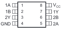
SN74 AUC 2G 00 DCU
SN74 is the typical prefix for these types of logic gates (there are other
groups that we'll ignore here).
AUC is the Advanced Ultra-low-voltage CMOS family. It works from 0.8V to
2.7V and its inputs tolerate a signal up to 3.6V.
2G means it packs two gates,
00 is the code for the NAND function,
DCU represents the physical package. It's pretty small, about 2mm x 3mm
with the leads.
It means these are dual NAND gates.
SN74 AUC 2G 02 DCU
These look a lot like the ones above, but they are dual NOR gates.
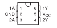
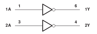
SN74 AUC 2G 04 DBV
04 is the numeric code for the inverter,
DBV is another package. That makes sense because inverters have only one
input, not two, so only six pins are needed to pack two of them.
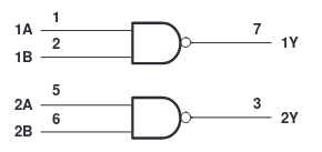
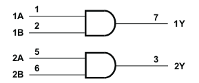
SN74 AUC 2G 08 DCU
We are back with some DCU packages, and 08 is the code for AND gates.
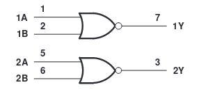
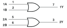
SN74 AUC 2G 32 DCU
You know the drill. Here, 32 means OR gates.
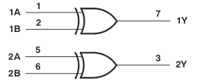
SN74 AUC 2G 86 DCU
And here is the last classic logic gates: the XOR gate, represented by the 86 code.
SN74 AUC 2G 53 DCU
Now, here is something new ! This is the famous analog FET switch that will
help us build various higher level blocks like the adder.
Here's how the datasheets presents it:
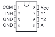
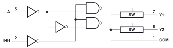
Admittedly, that logic diagram looks a bit more complex. Here's what it does.
It connects COM with either Y1 or Y2, depending on the input A. Unless the input INH is high, in which case COM is not connected to anything (both switches are open).
The key point is that the connection between COM and Yn is really just like a switch, meaning the propagation delay is very, very short. While it can take up to 2.2 ns to switch from one Y to the other, or to enable or disable the switch, it can transmit a signal in less than 0.1 ns !
This is the property that will help us build very fast chains, or ripple, as we have in adders or in AND gates with a lot of inputs.
SN74 AUC 1G 74 DCU
Only one gate in this package, as can be seen from the 1G part of the name.
74 is the code for a D-Flip-Flop.
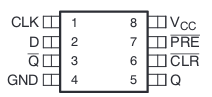
There's no reason to include the logic diagram for the flip-flop. I also won't explain how it works, I'm sure many people have already done so.
SN74 AUC 16 244 DGG
The 244 is nothing more than a buffer, or a driver, whose outputs can be
disconnected (tri-stated).
16 because that device is 16 bits.
DGG is the largest package available for this device, but don't be fooled.
The leads pitch is a mere 0.5 mm.
SN74 ALVCH 16 823 DGG
Here, we change family for a ALVCH device, for Advanced Low Voltage CMOS with
Hold. This can work with slightly higher voltage than the AUC, up to 3.6V. This
can be useful to drive the lines a bit stronger, for instance from board to
board.
Be aware that 16 is a trap, this part is actually 18 bits!
The 823 is a bus interface Flip-flop, with three usefull features:
- 3-state outputs,
- a clock enable pin, that can be used to prevent clocking in a new input value,
- an asynchronous clear pin, that set all outputs low independently of the clock.
I'm pretty sure various parts of our processor will make use of one or the other of the last two feature.
That's all
That's all the parts I've ordered this time, unless we count the thousand 100 nF
capacitors, and a mere hundred 10 nF ones :)
These are 0402 in imperial, or 1005 in metric. That means they are 1mm long by
0.5mm wide. This is the smallest size I have ever soldered by hand, and the
experience wasn't too painful.
Notes
The diagrams in this article have been copied from their respective datasheets and are © Texas Instruments Incorporated. The logic diagram for the dual XOR gate has been edited from the dual OR gate.
Links to the datasheets of the gates described above:
- https://www.ti.com/lit/ds/symlink/sn74auc2g00.pdf
- https://www.ti.com/lit/ds/symlink/sn74auc2g02.pdf
- https://www.ti.com/lit/ds/symlink/sn74auc2g04.pdf
- https://www.ti.com/lit/ds/symlink/sn74auc2g08.pdf
- https://www.ti.com/lit/ds/symlink/sn74auc2g32.pdf
- https://www.ti.com/lit/ds/symlink/sn74auc2g86.pdf
- https://www.ti.com/lit/ds/symlink/sn74auc2g53.pdf
- https://www.ti.com/lit/ds/symlink/sn74auc1g74.pdf
- https://www.ti.com/lit/ds/symlink/sn74auc16244.pdf
- https://www.ti.com/lit/ds/symlink/sn74alvch16823.pdf